- 您现在的位置:买卖IC网 > Sheet目录2004 > LTC1740IG#TRPBF (Linear Technology)IC ADC 14BIT 6MSPS 36SSOP
12
LTC1740
1740f
APPLICATIO S I FOR ATIO
WU
UU
Choosing an Input Amplifier
Choosing an input amplifier is easy if a few requirements
are taken into consideration. First, to limit the magnitude
of the voltage spike seen by the amplifier from charging
the sampling capacitor, choose an amplifier that has a low
output impedance (<100
) at the closed-loop bandwidth
frequency. For example, if an amplifier is used in a gain
of 1 and has a unity-gain bandwidth of 50MHz, then the
output impedance at 50MHz must be less than 100
. The
second requirement is that the closed-loop bandwidth
must be greater than 50MHz to ensure adequate small-
signal settling for full throughput rate. If slower op amps
are used, more settling time can be provided by increasing
the time between conversions.
The best choice for an op amp to drive the LTC1740 will
depend on the application. Generally applications fall into
two categories: AC applications where dynamic specifica-
tions are most critical and time domain applications where
DC accuracy and settling time are most critical.
Input Filtering
The noise and the distortion of the input amplifier and
other circuitry must be considered since they will add to
the LTC1740 noise and distortion. The small-signal band-
width of the sample-and-hold circuit is 80MHz. Any noise
or distortion products that are present at the analog inputs
will be summed over this entire bandwidth. Noisy input
circuitry should be filtered prior to the analog inputs to
minimize noise. A simple 1-pole RC filter is sufficient for
many applications.
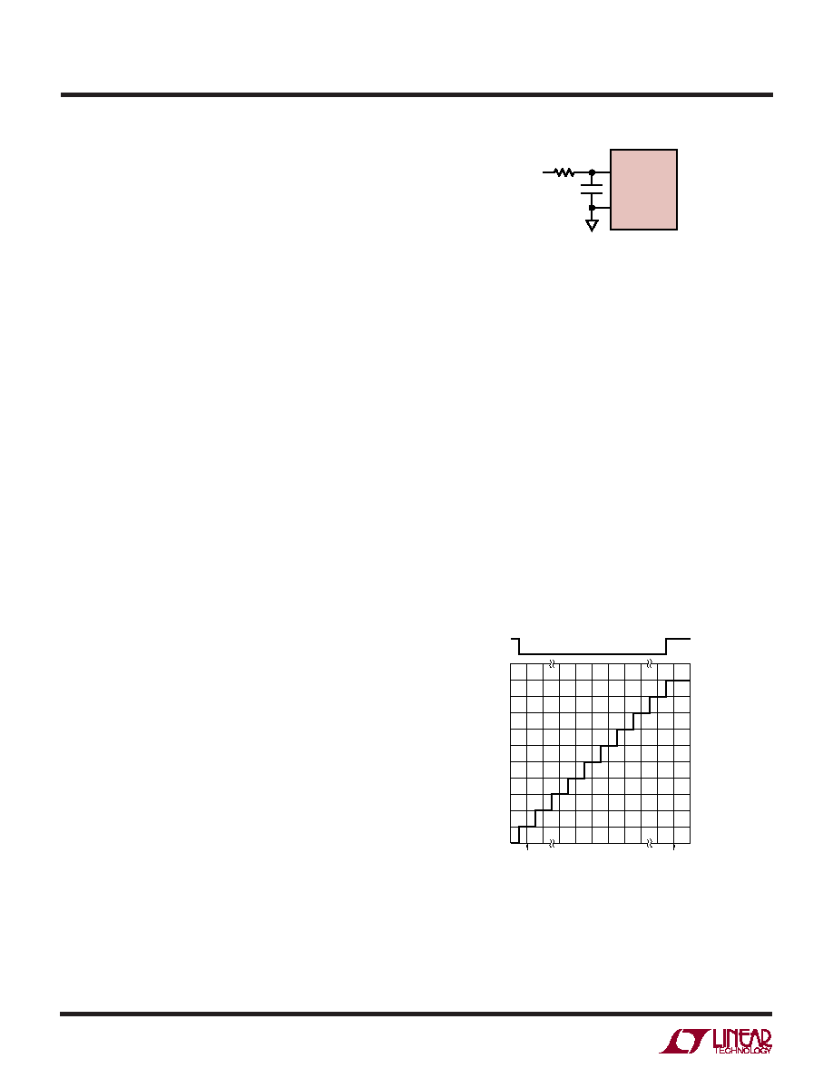
For example, Figure 9 shows a 1000pF capacitor from
+AIN to –AIN and a 30 source resistor to limit the input
bandwidth to 5.3MHz. The 1000pF capacitor also acts as
a charge reservoir for the input sample-and-hold and iso-
lates the amplifier driving VIN from the ADC’s small current
glitch. In undersampling applications, an input capacitor
this large may prohibitively limit the input bandwidth.
If this is the case, use as large an input capacitance as
possible. High quality capacitors and resistors should be
+AIN
VIN
LTC1740
1740 F09
–AIN
1000pF
30
Figure 9. RC Input Filter
INPUT VOLTAGE (V)
–(FS – 1LSB)
FS – 1LSB
OUTPUT
CODE
1740 F10
011…111
011…110
011…101
100…010
100…001
100…000
OVERFLOW
BIT
1
0
Figure 10. LTC1740 Transfer Characteristics
used since these components can add distortion. NPO and
silver mica type dielectric capacitors have excellent linear-
ity. Carbon surface mount resistors can generate distor-
tion from self-heating and from damage that may occur
during soldering. Metal film surface mount resistors are
much less susceptible to both problems.
Digital Outputs and Overflow Bit (OF)
Figure 10 shows the ideal input/output characteristics for
the LTC1740. The output data is two’s complement binary
for all input ranges and for both single and dual supply
operation. One LSB = VREF/(0.9 16384). To create a
straight binary output, invert the MSB (D13). The overflow
bit (OF) indicates when the analog input is outside the
input range of the converter. OF is high when the output
code is 10 0000 0000 0000 or 01 1111 1111 1111.
发布紧急采购,3分钟左右您将得到回复。
相关PDF资料
LTC1741IFW#PBF
IC ADC 12BIT 65MSPS 48-TSSOP
LTC1742CFW#TRPBF
IC ADC 14BIT 65MSPS 48-TSSOP
LTC1743IFW#PBF
IC ADC 12BIT 50MSPS SMPL 48TSSOP
LTC1744IFW#TRPBF
IC ADC 14BIT 50MSPS 48-TSSOP
LTC1745CFW#TRPBF
IC ADC 12BIT 25MSPS LN 48TSSOP
LTC1746IFW#TRPBF
IC ADC 14BIT 25MSPS LP 48TSSOP
LTC1747IFW#PBF
IC ADC 12BIT 80MSPS 48-TSSOP
LTC1748CFW#TRPBF
IC ADC 14BIT 80MSPS 48-TSSOP
相关代理商/技术参数
LTC1741CFW
功能描述:IC ADC 12BIT 65MSPS 48-TSSOP RoHS:否 类别:集成电路 (IC) >> 数据采集 - 模数转换器 系列:- 其它有关文件:TSA1204 View All Specifications 标准包装:1 系列:- 位数:12 采样率(每秒):20M 数据接口:并联 转换器数目:2 功率耗散(最大):155mW 电压电源:模拟和数字 工作温度:-40°C ~ 85°C 安装类型:表面贴装 封装/外壳:48-TQFP 供应商设备封装:48-TQFP(7x7) 包装:Digi-Reel® 输入数目和类型:4 个单端,单极;2 个差分,单极 产品目录页面:1156 (CN2011-ZH PDF) 其它名称:497-5435-6
LTC1741CFW#PBF
功能描述:IC ADC 12BIT 65MSPS 48-TSSOP RoHS:是 类别:集成电路 (IC) >> 数据采集 - 模数转换器 系列:- 产品培训模块:Lead (SnPb) Finish for COTS
Obsolescence Mitigation Program 标准包装:2,500 系列:- 位数:12 采样率(每秒):3M 数据接口:- 转换器数目:- 功率耗散(最大):- 电压电源:- 工作温度:- 安装类型:表面贴装 封装/外壳:SOT-23-6 供应商设备封装:SOT-23-6 包装:带卷 (TR) 输入数目和类型:-
LTC1741CFW#TR
功能描述:IC ADC SMPL 12BIT 65MSPS 48TSSOP RoHS:否 类别:集成电路 (IC) >> 数据采集 - 模数转换器 系列:- 标准包装:1,000 系列:- 位数:12 采样率(每秒):300k 数据接口:并联 转换器数目:1 功率耗散(最大):75mW 电压电源:单电源 工作温度:0°C ~ 70°C 安装类型:表面贴装 封装/外壳:24-SOIC(0.295",7.50mm 宽) 供应商设备封装:24-SOIC 包装:带卷 (TR) 输入数目和类型:1 个单端,单极;1 个单端,双极
LTC1741CFW#TRPBF
功能描述:IC ADC 12BIT 65MSPS 48-TSSOP RoHS:是 类别:集成电路 (IC) >> 数据采集 - 模数转换器 系列:- 产品培训模块:Lead (SnPb) Finish for COTS
Obsolescence Mitigation Program 标准包装:2,500 系列:- 位数:12 采样率(每秒):3M 数据接口:- 转换器数目:- 功率耗散(最大):- 电压电源:- 工作温度:- 安装类型:表面贴装 封装/外壳:SOT-23-6 供应商设备封装:SOT-23-6 包装:带卷 (TR) 输入数目和类型:-
LTC1741IFW
功能描述:IC ADC SMPL 12BIT 65MSPS 48TSSOP RoHS:否 类别:集成电路 (IC) >> 数据采集 - 模数转换器 系列:- 标准包装:1,000 系列:- 位数:12 采样率(每秒):300k 数据接口:并联 转换器数目:1 功率耗散(最大):75mW 电压电源:单电源 工作温度:0°C ~ 70°C 安装类型:表面贴装 封装/外壳:24-SOIC(0.295",7.50mm 宽) 供应商设备封装:24-SOIC 包装:带卷 (TR) 输入数目和类型:1 个单端,单极;1 个单端,双极
LTC1741IFW#PBF
功能描述:IC ADC 12BIT 65MSPS 48-TSSOP RoHS:是 类别:集成电路 (IC) >> 数据采集 - 模数转换器 系列:- 产品培训模块:Lead (SnPb) Finish for COTS
Obsolescence Mitigation Program 标准包装:2,500 系列:- 位数:12 采样率(每秒):3M 数据接口:- 转换器数目:- 功率耗散(最大):- 电压电源:- 工作温度:- 安装类型:表面贴装 封装/外壳:SOT-23-6 供应商设备封装:SOT-23-6 包装:带卷 (TR) 输入数目和类型:-
LTC1741IFW#TR
功能描述:IC ADC SMPL 12BIT 65MSPS 48TSSOP RoHS:否 类别:集成电路 (IC) >> 数据采集 - 模数转换器 系列:- 标准包装:1,000 系列:- 位数:12 采样率(每秒):300k 数据接口:并联 转换器数目:1 功率耗散(最大):75mW 电压电源:单电源 工作温度:0°C ~ 70°C 安装类型:表面贴装 封装/外壳:24-SOIC(0.295",7.50mm 宽) 供应商设备封装:24-SOIC 包装:带卷 (TR) 输入数目和类型:1 个单端,单极;1 个单端,双极
LTC1741IFW#TRPBF
功能描述:IC ADC 12BIT 65MSPS 48-TSSOP RoHS:是 类别:集成电路 (IC) >> 数据采集 - 模数转换器 系列:- 产品培训模块:Lead (SnPb) Finish for COTS
Obsolescence Mitigation Program 标准包装:2,500 系列:- 位数:12 采样率(每秒):3M 数据接口:- 转换器数目:- 功率耗散(最大):- 电压电源:- 工作温度:- 安装类型:表面贴装 封装/外壳:SOT-23-6 供应商设备封装:SOT-23-6 包装:带卷 (TR) 输入数目和类型:-